Status / throat clearing: Rough and incomplete working notes. They likely contains errors, misconceptions, and omissions; thoughtful, informed comments are welcome. I'm writing the notes as an experiment – I hope to get comfortable in quickly writing such working notes, and (frankly) for the quality to rise a lot.
When growing up I read in some well-meaning-but-wrong book that human beings had no way to see individual atoms. I thought this was amazing: somehow, we knew matter was made up of atoms, despite not being able to see them. I used to hold the palm of my hand up close to my eyes and squint, hoping I'd be able to make out individual atoms, or at least individual cells. I sometimes fancied I saw something, but was never quite sure what.
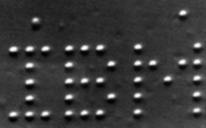
In fact, what I'd read was wrong: human beings have had multiple ways of seeing atoms for decades. One fascinating approach is the scanning tunneling microscope (STM), invented in 1981 by Gerd Binnig and Heinrich Rohrer at IBM Zurich. Indeed, not only can STMs see individual atoms, they can also be used to manipulate atoms. This was done by Don Eigler and Erhard Schweizer at IBM Almaden, who in 1989 used an STM and 35 xenon atoms to spell out "IBM" on a nickel surface:
Since that time, STMs have been used to do many things, including to study at the single atom level exactly how certain catalytic reactions work, and even to design new catalytic reactions.
While today we have many different ways of “seeing” atoms, I've never dug down into the details of how any of these approaches work. In these notes I explore how STMs work, what some of their limits are, and how they might be improved. Of course, the STM is just one way of interrogating the nano-world, and there are many others. Still, it seemed a good place to start.
The basic idea: Let me outline the very basic idea of how STMs work, leaving details for later. An STM has a very sharp conducting tip, which is placed a few angstroms above a 2-dimensional surface, and a voltage is applied between the tip and the surface. When the tip is held this close to the surface there can actually be a tunneling current between the surface and the tip, despite the lack of any conducting material between them. That tunneling current depends on the charge density on the surface of the material. And so by carefully measuring the tunneling currrent it is possible to infer things about the surface: the tunneling current is, effectively, a microscope giving us a view of the surface (at least, the electronic properties of the surface).
Here's a diagram showing how an STM operates, from a book by C. Julian Chen*C. Julian Chen, Introduction to Scanning Tunneling Microscopy" 2nd ed (2008). There are many elements in this diagram, and you perhaps won't take it all in at once. I'll explain some of the elements later in the notes. For now, it's worth noting the flat sample, the sharp tip just above it, and that the current from the tip goes through an amplifier and is ultimately fed to a computer where it is used to extract a signal, i.e., it's used to see the surface.

The description of how STMs work given above is fine, as far as it goes. But it leaves unanswered a lot of questions. How sharp does the tip need to be? How can we place the tip close to the surface in a stable way, without it shaking too much, or being broken? Why is it a tunneling current which is measured, and not just an ordinary current? What's meant by a tunneling current, anyway? Does the tunneling current perturb the surface so much that the image is unreliable? What information do we actually get out of the tunneling current? And what is invisible to the STM?
And so on: there's an absolute tonne of questions! I know only a little about the answers, but we'll get into it through the remainder of these notes, hopefully while having some fun along the way.
Image of an early STM device: Let's take a look at an image of an early STMImage due to user Rama on Wikipedia.:

It's a historic STM, from 1986, a few years after the very first STM (in 1981). It's hard to tell the scale from the image alone, but it was the size of a small tabletop.
I find such images fascinating but frustrating. They're a bit like museum displays – the trouble with museums is that you often know that what you're seeing would be utterly fascinating if only you had eyes to truly see it. But you usually lack those eyes. You see something very mundane – dining implements or cups or whatever, and you know they must have played an important role in the life of some household, and perhaps of some craftsperson. You'd love to hear stories from all those people – how the items were made, how they were used in everyday life, and so on. But most of that context is lost to you. And the best you can do is try to infer some of that context by looking closely** I had dinner once with a museum curator. And he was just fascinating: he could talk in depth for hours about many such items. It made me wonder how much context could be supplied for museum exhbits, but isn't. One of my favorite museums is the (decomissioned) USS Midway Aircraft Carrier in San Diego. Part of what makes it so fascinating is that many former crew members volunteer at the museum, and so you can hear directly what it was like to live and work on the ship. Of course, those crew members are getting older, and I recommend going while as many as possible are still telling their stories..
It is similar with images of scientific equipment. You can guess the STM shown above was someone's life for years. Likely every single element of the device was deeply important and meaningful to one or more people. But all that context is stripped out of the photo, and needs to be inferred.
Here's four things that stand out to me.
First is the four micrometer screw gauges, presumably used to accurately position objects. They're not nearly accurate enough to exactly position the STM tip, so I'm not sure what they're being used for – presumably it was to do rough positioning, either of the tip or the sample.
Second is the chunky metal construction. This thing looks solid. I suspect, though don't know, that simple solidity may have been a helpful part in getting vibration isolation and stability.
Third is something I don't see: I don't see much sign of cooling or of vacuum equipment. My understanding is that modern STMs often operate at cryogenic temperatures, and in vacuum. Maybe that was done here, and is just not shown. But it makes me wonder if early STMs didn't need that?
Four, I can't help but smile at the mess of wires and makeshift construction. That's tabletop experimental physics – if things look too neat, something was either bought from a commercial supplier, or not much is going on. Experimental physicists are astoundingly good at repurposing and generally jury rigging stuff to do amazing things. Love to see it!
Listening to a surface: Earlier, I mentioned Don Eigler – one of the people behind the IBM Xenon atom image. One of the highlights of my life was in the late 1990s, when I visited Eigler's lab at IBM Almaden. I met Hari Manoharan, who at the time was the postdoc running many of the experiments in Eigler's lab.
As I recall the way he explained it (errors my own): Hari had noticed that as he manipulated the tip of the STM he was often glancing at a screen to monitor the tunneling current. He decided that was wasteful, since it took his eyes off the equipment in front of him. Instead, he installed a (gigantic) audio speaker in the ceiling above the table, which he used to amplify the tunneling current to produce a sound. He'd learned how to listen to the surface. I wish I'd thought to ask him, but it was clear in some sense he could hear what an atom sounded like, and different features on the surface** Somewhat related: a moment I enjoy in John Boswell's marvellous Timelapse of the Future is when he shows black holes orbiting and plays an audio analogue (I don't know how accurate) of the gravitational waves produced by those orbiting black holes, the sound of “black holes singing”..
How do you position the tip? Typically, the tip is no more than a few angstroms away from the surface being measured. That's really close! How do you position it there, and keep it stable?
The basic idea is to use the piezoelectric effect. If you run electricity through certain materials – often, though not always, crystals – they deform slightly in shape. The reverse is also true: if you push on the piezo materials a bit, they generate electricity. The effect is quite small – you can run a fair bit of current through the piezo material and it will only change shape a little. Furthermore, it's very repeatable and reversible: turn the current off and it returns to its original shape; turn the same current back on, and you'll get a similar deformation.
Piezoelectricity is used in many places: it's used for instance in cigarette lighters, loudspeakers, barbecues, guitars, quartz watches, inkjet printers, and (I love this) potato cannons. Being able to convert mechanical change into electricity, and vice versa, is useful!
If you've ever operated a cigarette lighter you were very likely operating a piezo crystal. When you push down on the lighter's button, that mechanical motion is used to push on a piezo crystal, compressing it slightly. That produces electricity, creating a spark which ignites the fuel. Clever!
For the purpose of STM, the main thing is that everyday electric currents produce only tiny (and very predictable and stable) changes in the size of the piezo material. That allows you to control the placement of the tip at the atomic level(!!!) In fact, three piezo crystals are used, to control movement in the x, y, and z directions. Conventionally, two of those are chosen to form a plane parallel to the (very near atomically flat) sample, while the third direction controls the height above the sample. Typically, a voltage ramp is applied to the x and y piezos, so the STM "scans" back and forth over the sample, creating a raster image.
All that said, I understand poorly how most of this works. Here's a few of the more important questions I'd like to understand the answers to.
Most of all: I just don't understand the mechanism of piezoelectricity very well. Why should relatively large currents only produce nanometer-scale deformations, and do so in a very predictable, very repeatable way? I presume this requires tremendous stability on the part of the piezo material. Can't that stability be very easily interrupted? Why isn't it destroyed if a cosmic ray zips through? Or if a truck drives past?
Speaking of stability: if you're going to hold the tip of something a few angstroms above a surface, you need to worry a lot about vibrations. Try holding a pencil a millimeter above a surface for 10 seconds. You can likely do it (unless your hand trembles). Then try doing it a tenth of millimeter. I suspect for most people that's pretty difficult – it's getting down to the limits of our muscles' ability to do control.
Of course, the problem for STMs is far worse. In particular, you'd expect nearby vibrations (e.g., a truck driving past) to cause both the STM tip and the surface being probed to vibrate. The trouble is: why should they vibrate in exactly the same way? After all, they're typically made of different materials, which will respond in different ways to vibration (think of the fact that different drum materials sound quite different). And if they respond in different ways then isn't it likely the STM tip would sometimes bash up against the sample, and sometimes be too far away from the sample?
I know a little about how labs protect against this – the basic trick is to isolate experiments from environmental vibrations. You can see that in the image above from Chen's book – hanging the entire experiment on a spring. A closely related trick is to float laboratory tables on air. But I don't really understand how it works, not in detail.
Obvious things to wonder about include: (1) the fact that there still will be coupling out from the STM, apart from the spring. Vibrations through the wires to the computer (and similar) will be small, but the STM tip and sample need to be positioned to angstrom-level accuracy. So even very small vibrations are potentially a problem. And: (2) it's not obvious the spring will couple in quite the same way to the STM tip and to the surface. That's potentially a problem.
All this may seem like details, but they're details at the heart of much of modern science and technology. I may write some future notes digging much more deeply into piezo materials and into stabilization and vibration isolation.
On the microscope tool pattern: Microscopes let you see the ordinarily unseeable. They do it through some combination of amplification of signal, and suppression of noise. Of course, this is a very broad definition, perhaps too broad: taken literally it identifies telescopes, PCR, hearing aids, and many other things as “microscopes”. Still, these patterns – amplification and noise suppression – are ones to be very aware of – whenever they're identified, there's the possibility to build a new type of microscope. And: “can we build a new type of microscope?” has been an astoundingly productive question in science. It's how we see the world.
Learning to see also helps us to do. It's sometimes said that an actuator is just a microscope run backward. In particular, when we have good de-amplifiers it means we can take gross actions in the human world, and turn them into movement inside the microscopic world.
I'm a little uncomfortable with my use of “amplifier” and “de-amplifier” above. Those are the right terms in many cases. But there's really a broader pattern, which has nothing to do with the relative size of the input and output signals. Rather, it's just about converting signals from one domain to another. A piezo material converts electrical signal into mechanical motion; it can also be run the other way to convert mechanical motion into electrical signal. PCR uses a series of such transformations to ultimately converts tiny differences in genetic material into large differences in electrical signal. An STM uses a series of such conversions to turn a tiny fluctuation on a surface into a (large) electrical signal** Programmers sometimes note that much of the work in complex code bases is often about converting things from one data format to another. I'm struck by the similarity, though not sure what to make of it.. It's not so much the size of the signals that matter (though it often does), but merely the possibility of converting from one domain to another.
A striking difference between STMs and optical microscopes: in an optical microscope there's no need to accurately position a tip (though coarse positioning is still needed). Instead, you grind a lens which focuses rays in an image plane; the image is a magnified version of the original. Furthermore, the lens can sustain a certain amount of imperfection, although the overall shape must be correct, and the material quite pure; in some sense the magnification is a collective effect. If anything, the lens is most closely analogous to the amplifier that turns the (tiny) current in the tip into a signal we can see. And there is nothing in an optical microscope analogous to the tip. Are there approaches to microscopy that don't have at their core either an amplifying lens or a very accurately positioned tip?
Other questions: Let me conclude by enumerating a few other questions, some of which I may come back to in future notes:
Practically, I'd like to fill in many gaps. I'd love to know how the very sharp conducting tip is made – it's pretty astounding! And I'd like to understand the entire chain of ways in which the tunneling current is amplified – it's apparently on the order of nanoamperes (surprisingly large, in my opinion – that's millions of electrons per second).
I haven't talked about theory at all – of course, underlying all this is detailed theoretical models of STMs. Questions I'd be particularly keen to dig into: what are the limits to the resolution? Doesn't this disturb the surface? How large is the disturbance caused? How well can we probe beneath the surface? Could you do this with something other than electrons? And what's invisible due to the reliance on electrons?
Longer term, I'd love to know what else we can do with this set of ideas. Is it possible to fabricate a regular array of closely packed STM tips and use them to image (and manipulate) a large surface? Might there be some way of doing it in 3d? It seems hard – there's a lot of barriers, but maybe with some imagination it'd be possible to image, and perhaps even to manipulate, large numbers of atoms in 3d using techniques derived from STM.